
Tesla Three
Principle of operation
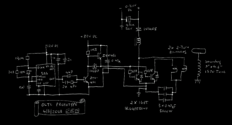
When I designed Tesla Three, I basically took a standard DC resonant charging circuit and modified it a bit.
Preliminary schematic
Power circuitry
Of course, the finished article is going to run off the rectified AC line. To make my life safer, though, I powered the prototype with an 0-300V regulated bench power supply. The DC supply feeds through a diode and a choke into the tank capacitor. Twin 50-amp IGBTs then fire the power into the primary coils, just as the spark gap in a conventional Tesla coil does. Note, the IGBTs can't just be connected in parallel. To ensure that they share current equally, two separate tightly-coupled primaries are used. The two IGBTs are mounted physically as close together as possible and the emitter terminals are connected together using a thick and short jumper wire. All other connections, including the ground return for the gate drive signal, are taken from the middle of this jumper. The object is to minimize and equalize parasitic inductance in the two emitter current paths. If this is successful, then both IGBTs should be able to share a single gate drive signal with no problems. Otherwise, two separate transformer-isolated gate drives would be required.
Note: Power MOSFETs always have an internal diode between source and drain. It's part of the device whether you like it or not. On the other hand, IGBTs can be bought with diode or without. The diode is a separate silicon chip added in ("co-packaged") at the factory. For this circuit, you want them with diodes. For instance, International Rectifier part# IRG4PF50WD (the D stands for diode) The reason I'm labouring this point is because I didn't know and bought a bunch of IGBTs without diodes.
Timing circuit
The timing circuit is pretty standard, made from a 555 timer in astable mode. In this version, the break rate is fixed at about 80bps due to power supply limitations. The finished model will be adjustable between 20 and about 1000 bps. There is a trimmer to set the "on" time and hence quenching properties. I experimented with automatic first-notch quenching, but abandoned it because:
- it was too difficult to detect the notch, and
- if the coil is sparking, all the energy is gone by the time of the first notch anyway. If it doesn't spark, then it might as well just blow up.
So I went for manual adjustment instead. I run the coil at low voltage and adjust it with a scope so that it quenches at the third notch. I intend to try modifying the driver so that it always turns off at a current zero, failing that, a couple of transzorbs across each IGBT will protect them from kickbacks. However, modern IGBTs have controlled avalanche and can probably soak up more energy than the transzorbs anyway...
In a future revision I hope to synchronise the turnoff with the times when the current is negative and the co-pack diode is conducting. This is the best time for turnoff because the current through the actual IGBT is zero and the voltage across it is zero too.
Gate drive circuit
The gate drive circuit is one I designed myself. I need this because the IGBT has to be driven with 30 volts or more, but a 555 can only give out 16 volts before it blows up. I used the special ZTX451 transistors which can give pulsed current up to 2 amps. With the speedup network between the 555 and the first transistor, it turns on and off in about 300ns. This is slow compared to state-of-the-art gate driver chips, but plenty fast enough for our application.
OLTC design issues
Here we come to the main problem, oops I mean design challenge, with the OLTC. The tank capacitor can only charge to twice the line voltage. (You could devise a circuit that charged it higher, but the breakdown voltage of available IGBTs limits you to about 700V anyway.) Therefore, you have to make the capacitor very large in order to store a reasonable amount of bang energy. This in turn means that the secondary has to have a very low resonant frequency, and also that the primary will only be 1 or 2 turns. Therefore, the primary surge impedance will be low, and huge currents will flow.
In this design, I adopted several ways of dealing with this.
- Firstly, I made the whole coil pretty small (9" x 4.5").
- Secondly, I made the secondary with as many turns as I could (1500).
- Thirdly, I used the largest IGBTs I could afford, and overdrove them with excess gate voltage, a technique pioneered by the original OLTC inventor, Terry Fritz.
- Fourthly, I made the primary in the form of two tightly-coupled coils, with each coil driven by a separate IGBT. The coupling forces equal currents to flow in the coils by transformer action, and hence each IGBT takes half the current. This technique could be extended to parallel any number of IGBTs but I reckoned two would be enough. The original OLTC inventors did something similar, but splitting the capacitors instead of the coils.
- Finally, I used a high break rate. The prototype is adjustable and should operate at least 400bps, hopefully up to 1000bps if the heating does not prove to be a limiting factor.
Return to TC Page